When buying memory, selecting dies, or tuning for overclocking, the most common question is: what die is actually used on this module?
This article organizes a reusable identification workflow around three common vendors: Samsung, Micron, and SK hynix. The examples here are mainly DDR4.
Start With the Method
- Check the full on-chip marking and complete part code first.
- Cross-check with official vendor lookup tools.
- Use forum tables and community experience only as the final layer.
If you rely only on software detection, or only on one letter in the code, misidentification is very likely.
Samsung Dies
1) Naming Rule Diagrams
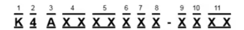
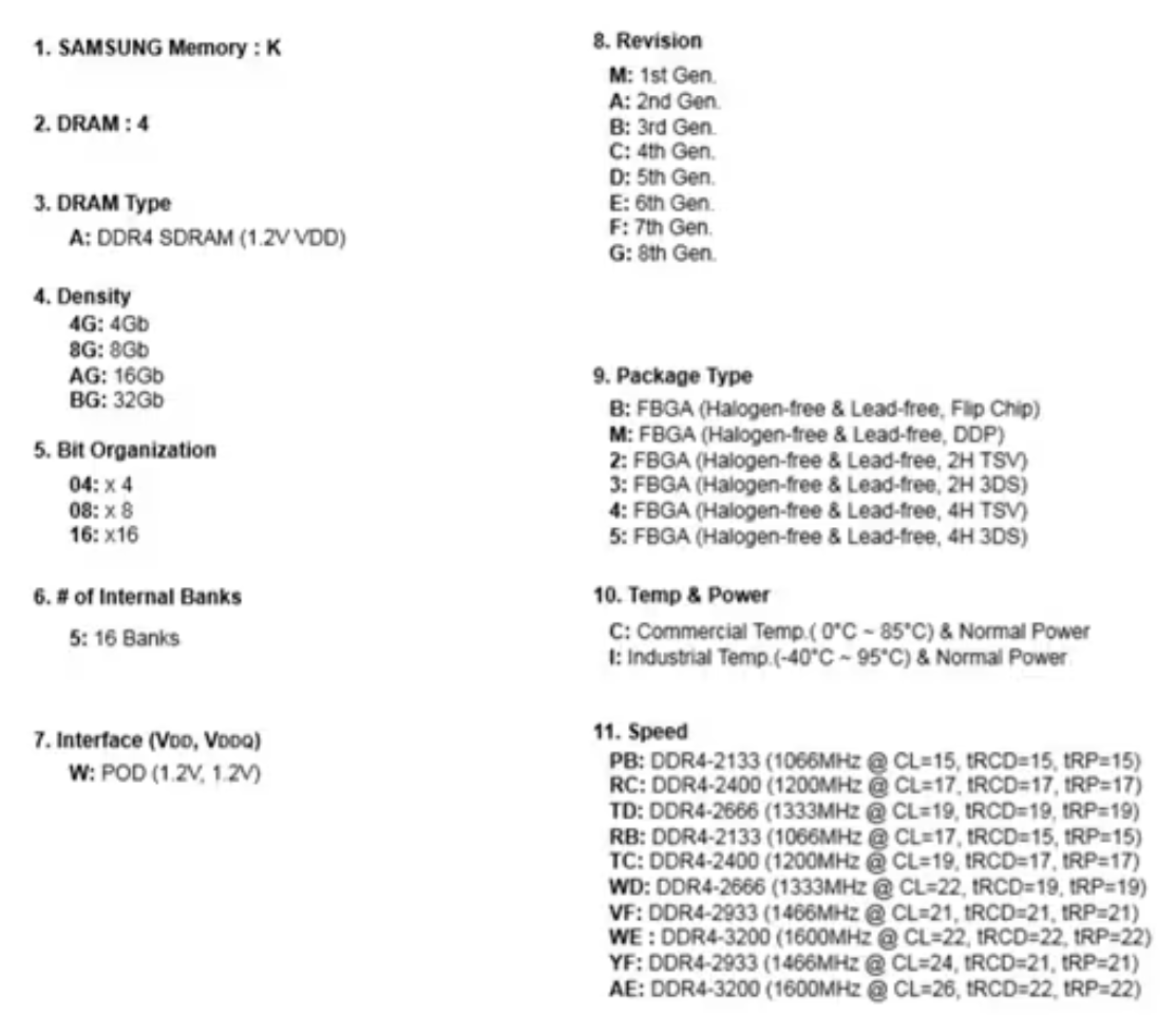
Common readable fields in Samsung DDR4 die codes:
- Vendor prefix:
K - DRAM class:
4 - Generation:
A = DDR4 - Density:
4G/8G/AG/BG=4/8/16/32Gb - I/O width:
04/08/16=x4/x8/x16 - Revision generation:
M/A/B/C/D/E/F/G - Speed bins: commonly
PB/RC/TD/...
2) Real Sample
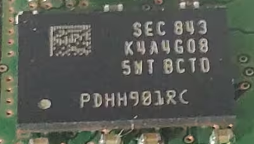
Sample breakdown:
- Line 1
SEC 843: commonly indicates production batch info. - Line 2
K4A4G08:4G08commonly maps to density/width. - Line 3
...TD:TDcommonly maps to DDR4-2666 CL19. - Line 4 corner mark: useful as reference, but should not be used as the only conclusion.
Micron Dies
1) Marking Layout and Sample
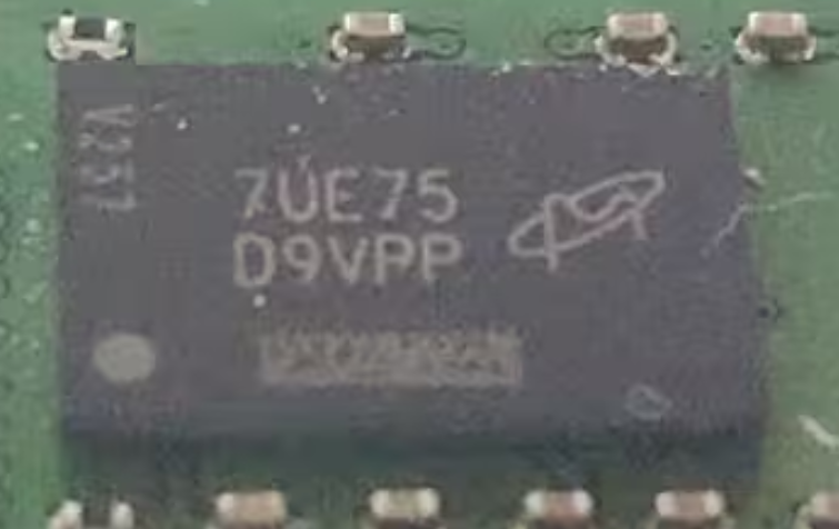
Using 7UE75 / D9VPP as an example:
7UE75can indicate date batch, revision, and diffusion/assembly location info.D9VPPis the FBGA code, and should be checked in the official tool next.
2) Official FBGA Lookup
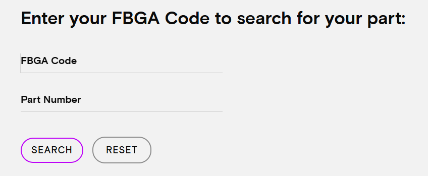
Lookup URL:
3) Part Number Mapping
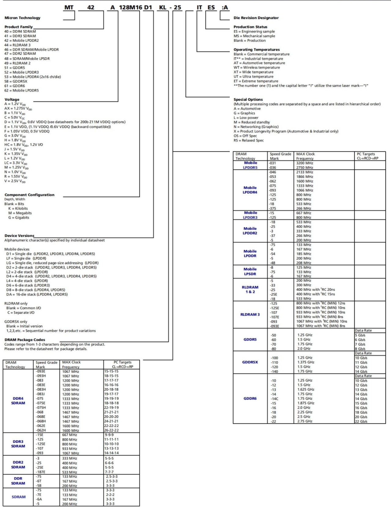
Sample: MT40A1G8SA-075:E
40: DDR4 family1G8: 8Gb x8512M16: 8Gb x16075: commonly maps to DDR4-2666 CL19083: commonly maps to DDR4-2400 CL17093E: commonly maps to DDR4-2133 CL15E: maps to E-die revision
Spectek (Large-S, Micron White-Chip Line)
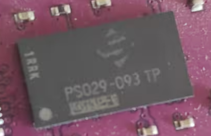
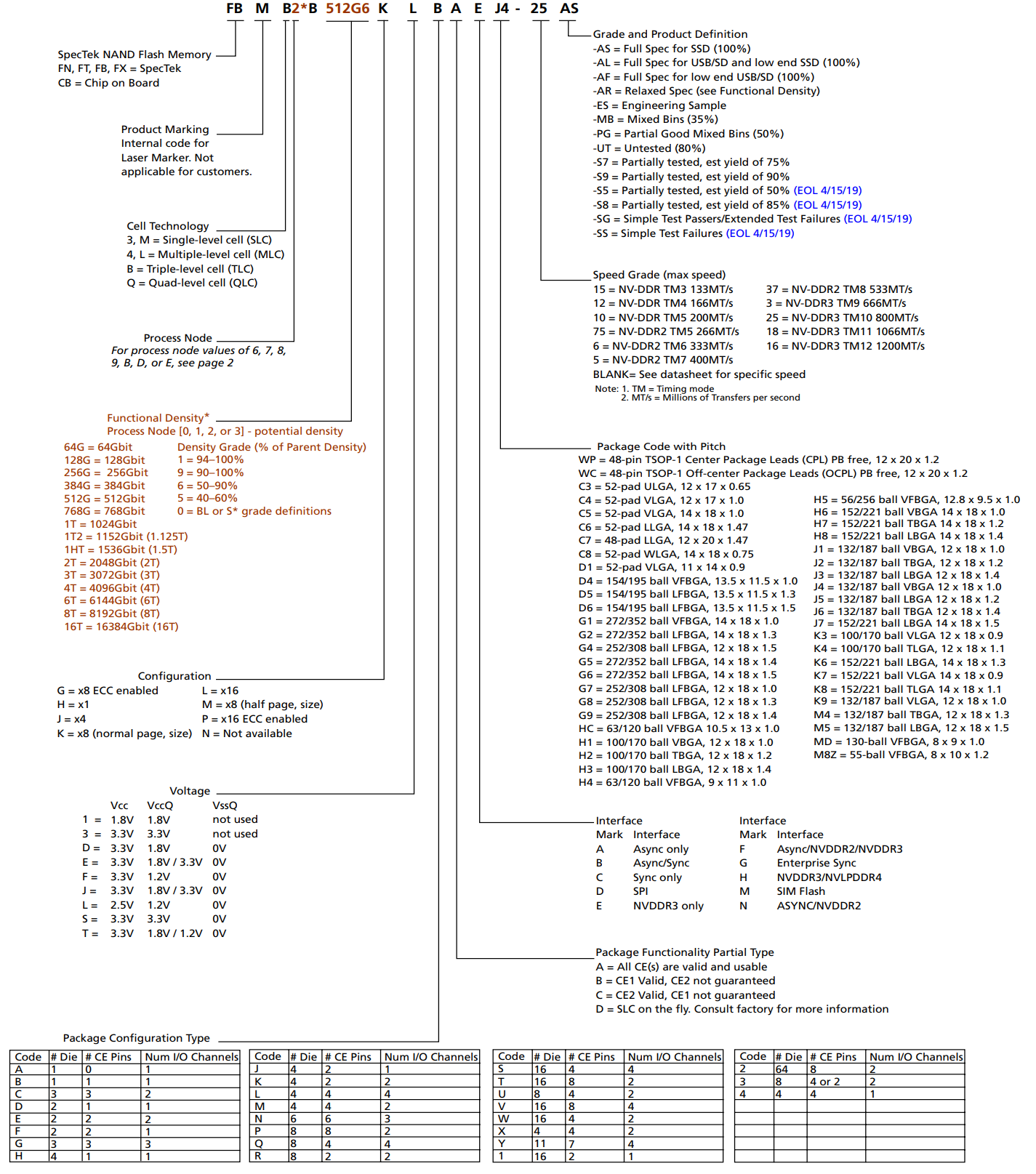
Common format: PS029-093 TP
PS029: can be queried on the Spectek website.093: commonly maps to a speed/timing bin.TP: commonly used as a quality grade mark.
Lookup URL:
SK hynix Dies
1) Naming Rule Diagrams
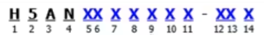
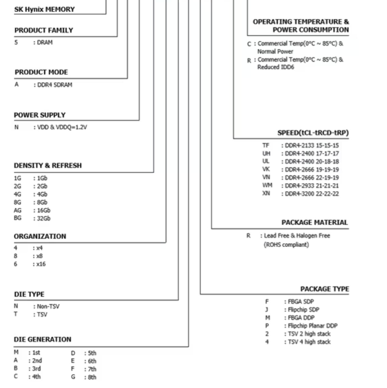
Common readable fields in SK hynix DDR4 codes:
PRODUCT FAMILY:5 = DRAMPRODUCT MODE:A = DDR4 SDRAMPOWER SUPPLY:N = VDD/VDDQ 1.2VDENSITY:1G/2G/4G/8G/AG/BGORGANIZATION:4/8/6=x4/x8/x16DIE TYPE:N = Non-TSV,T = TSVDIE GENERATION:M/A/B/C/D/E/F/GSPEED:TF/UH/UL/VK/VN/WM/XNPACKAGE TYPE:F/J/M/P/2/4- Temperature/power flag:
C,R
2) Real Sample
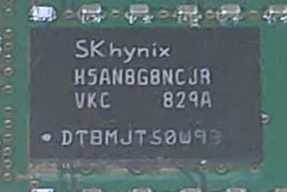
Sample H5AN8G8NCJR:
8G8: commonly means 8Gb x8.C: commonly used for C-die generation identification.VK(visible on the next line): commonly maps to DDR4-2666 19-19-19.- Tail batch code (for example
829A) can help estimate production timing.
Common Pitfalls
AFR/CJR/MFRare common community names, but not the full official definition.- The same memory model may change die source across production batches.
- With white chips, relabeled chips, or mixed batches, software-only detection is error-prone.
References and Notes
- This article is for hardware education and troubleshooting, not a purchase guarantee.
- Final identification should be based on physical markings and official lookup results.
- Reference (compiled): https://www.bilibili.com/read/cv2519652/?opus_fallback=1
- Official tools (lookup/reference):
- Micron FBGA: https://www.micron.com/support/tools-and-utilities/fbga
- Spectek Mark Code: https://www.spectek.com/menus/mark_code.aspx
- Spectek reference page: http://am.adianshi.com:6805/%E5%BC%80%E5%8D%A1%E8%BD%AF%E4%BB%B6/%E6%96%87%E6%A1%A3/spectek_flash.pdf