Typical Crystal Oscillator Circuit
A typical crystal oscillator uses two external capacitors with equal values (C1, C2). They are often called matching capacitors (or load capacitors in common usage).
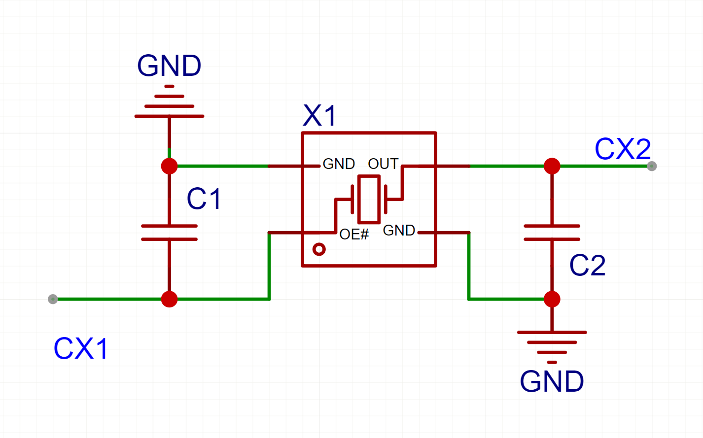
Datasheets usually specify a required load capacitance CL (Load Capacitance), which is the effective capacitance seen by the crystal.
If load capacitance is too large, oscillation frequency tends to shift lower. If too small, frequency tends to shift higher.
Parasitic Capacitance and Calculation
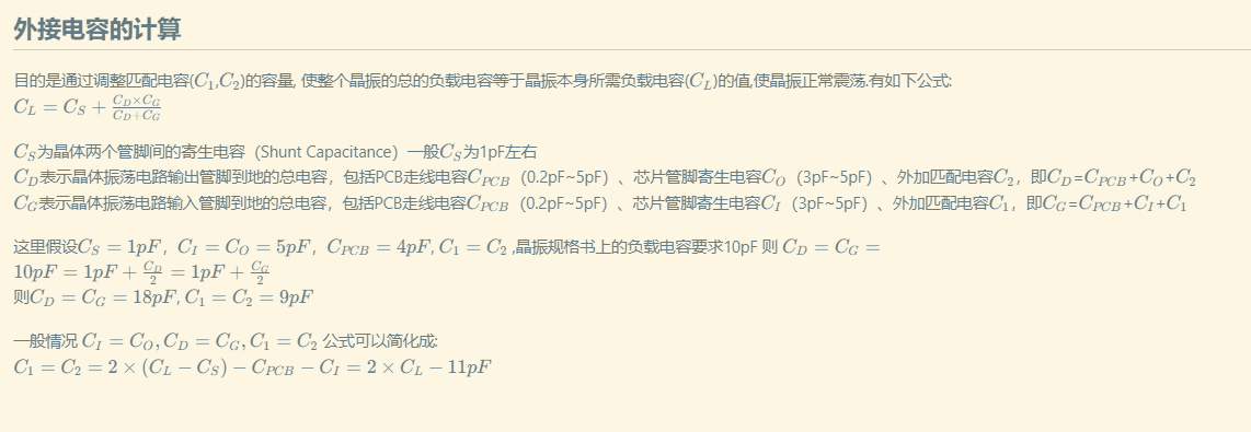
Goal: choose matching capacitors (C1, C2) so the crystal sees its required CL.
Formula:
${C_L}={C_S}+\frac{C_D \times C_G}{C_D + C_G}$
Where:
CS: shunt/parasitic capacitance (often around 1 pF in rough estimation)CD: total capacitance at one crystal pinCG: total capacitance at the other crystal pin
Common expansion:
${C_D} = C_{PCB} + C_O + C_2${C_G} = C_{PCB} + C_I + C_1
CPCB is PCB stray capacitance, CI/CO are MCU internal pin capacitances.
Example
Given:
${C_S}=1pF${C_I}={C_O}=5pF${C_{PCB}}=4pF${C_1=C_2}- crystal requires
${C_L}=10pF
Then solve to get approximately:
${C_D=C_G=18pF}${C_1=C_2=9pF}
Under symmetric assumptions (CI=CO, CD=CG, C1=C2), a simplified form can be used.