Dual Power Automatic Switching Circuit (Near-Zero Drop)
A key advantage of this design is very low conduction drop, making it suitable for battery-powered and low-loss power-path applications.
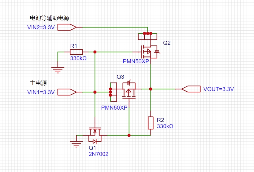
This circuit uses MOSFET switching behavior and low Rds(on) characteristics to achieve automatic source selection.
Circuit and Functional Behavior
- When
Vin1 = 3.3VandVin2is absent,Vin1suppliesVoutthrough the MOSFET path. - When
Vin1is removed, the circuit automatically switches soVin2suppliesVout. - Because selected MOSFETs have low
Rds(on), voltage drop is typically only tens of millivolts. - With a single source active, quiescent current is around the microamp range, suitable for low-power systems.
Principle of Operation
- With
Vin1 = 3.3V, NMOSQ1turns on, pulling gate conditions such that PMOSQ3conducts and PMOSQ2is off. Output is supplied fromVin1. - When
Vin1is removed,Q1turns off. Bias network drivesQ2on andQ3off, so output is supplied fromVin2.
For practical design, choose MOSFETs with:
- low gate-threshold voltage
- very low
Rds(on)at target gate drive voltage
Example device notes from the original design:
Q2 = Q3 = PMN50XP(lowRds(on)around 3.3V gate drive)Q1can use2N7002
Final selection should be based on required current, voltage, and thermal budget.